|
|
| Elliott Sound Products | Opamp Alternatives |
 Main Index
Articles Index Main Index
Articles Index
|
In the field of audio, there are many people who, for one reason or another, dislike opamps (operational amplifiers, aka op-amps). In some cases there is almost a passionate hatred, despite the vast number of extraordinary opamps available. Some have been around for a long time, and although they replaced the circuits described in this article in 99% of all equipment, it is worth looking at the circuits that were used in the pre-opamp (but post valve/ vacuum tube) years.
The earliest circuits used circuitry that was very similar to that used in the valve era - simple, single stage amplifiers with little or no feedback. These could not hope to compete with valves because of the huge supply voltage difference - valve circuits operating with 200V supplies cannot be compared to a transistor circuit using a 20V supply if the same signal level was expected. 1V RMS is nothing compared to 200V - it's less than 1.5% of the supply voltage with a valve, but over 14% with a transistor having a 20V supply.
In addition, valve design was at its peak, and electronics designers were very used to creating circuits that were optimised in every respect. Early transistors were mediocre by modern standards, designers weren't used to working with these 'new fangled' devices, and there was a great deal that had to be learned. Of course valves sounded better!
As we progressed, new arrangements were devised that while more complex than the early stages, had performance that could not be matched by any earlier circuits (including valves). Of the improved circuits, Philips was responsible for many of the two transistor feedback amplifiers that became commonplace in hi-if equipment of the day. There is no denying that the performance of some of these circuits is/ was very good indeed (usually far better than valves), but it is exceeded in most respects by even low-cost opamps available now.
This article cannot even hope to show all the variations, but the most common circuits are examined. This is an excellent way to learn more about transistors, how they work, and what you can do with them, and as such is recommended reading for anyone who is learning electronics or wants to brush up on what is now an 'ancient technology'. One of several things that isn't covered in detail is noise. Valve circuits were usually comparatively noisy due to the high resistances involved, and these contribute thermal (white) noise (see Noise In Audio Amplifiers). All amplifying devices also contribute some noise, so in the valve era it wasn't uncommon to see transformers used to boost the voltage without excess noise (note that a transformer is not an amplifier).
For most examples, an output voltage of 2V RMS will be used - this is for no other reason than to be able to show the difference between the circuits and to give a reasonably good idea of their relative performance. For the same reason, a supply voltage of 18V was chosen for all single-supply circuits that follow. Likewise, the gain has been set to 10 (or as close as standard value resistors will allow). This is a voltage gain of 20dB. All circuits are loaded by 10k, again for repeatable results. This is also a reasonably representative load - perhaps a little on the low side, but chosen to give the most realistic result available from the SIMetrix [ 1 ] simulator (or any simulator for that matter).
Where DC voltages are needed for understanding circuit operation they are shown in red. In most cases the description and/or simple semiconductor basics are enough to work out the voltages. In general, assume the emitter-base junction voltage to be between 600 and 700mV. Some voltages have been rounded to the closest sensible value, so do not assume they are exact, because they aren't. If you build the circuits, the voltages won't be exact either.
Bipolar junction transistors (BJTs) have long been the preferred 'solid state' device, partly because they were the first available, and largely because the technology advanced quickly, first germanium, then silicon, and ever more sophistication in terms of fabrication and performance. The simplest of all transistor amplifiers, single transistor designs were common in the very early days of transistor applications. They are very limited even today, and were much more limited when only germanium transistors were available. Unlike a valve (vacuum tube), input impedance is relatively low - this caused many of the early designers some grief because so many of the sources were high impedance.
There are ways around anything, but noise performance was usually rather ordinary - in some cases worse than that obtained from valve circuits. However, the overall convenience of equipment that could be operated from a single (low voltage) battery was just too overwhelming, and the days of the valve were numbered when Sony released one of the first of all transistor portable radios. This early radio was reliable, and had surprisingly good performance (germanium transistors, remember). Yes, I did have one. 
The circuits in Figure 1 became the standard for single transistor amplification stages. There are other variants, but they either have poor thermal stability or poor tolerance for different transistor gains (or both). The single resistor bias shown has worse stability for temperature and transistor differences than 'conventional' bias. The two circuits shown are classified as 'common emitter', because the emitter is at (or near) ground for both input and output signals.
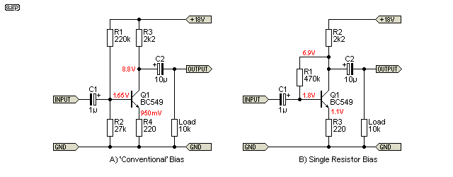
The drawing above shows two versions of a capacitor coupled AF (audio frequency) stage. Although transformer coupling was also used on occasion this was usually restricted to RF circuits or simple low power speaker amps. There were some instances where transformer coupling was used for audio, but the demands for lower cost and better performance saw the demise of transformers in this application. Transformer coupled audio stages will not be covered.
As always, these 'simple' amplifiers are almost always biased so that the collector voltage is about ½ the supply voltage, so in the examples above (audio frequencies only) the collector voltage is set to about 9V. Both versions perform similarly with a low impedance source, but only the (A) version will be analysed here. The (B) version is fairly common, but is more sensitive to variations in temperature and/ or the transistor's gain than the 'conventional' bias system. The collector voltage of the (B) version is lower than desirable.
With the standard load of 10k, the Fig 1 (A) amp has a total harmonic distortion of 0.218% - not too shabby, but several orders of magnitude worse than even an 'ordinary' opamp. The output FFT spectrum is shown in Figure 2 - low order harmonics predominate, and it is worth noting that 1µV referred to 2V peak output is -126dB. This is well below the noise floor that can be expected for this type of circuit.
The basic amplifier has many disadvantages. Input impedance is rather low, and is only 16k for the (A) circuit as shown - it's higher for the (B) version, but is a great deal harder to calculate. Output impedance is equal to the value of the collector resistance (2.2k in this case), and the local feedback provided by the emitter resistor does not affect this. Stage gain is (approximately) equal to the collector resistance divided by the emitter resistance. For the two examples shown the gain is actually only 7.95 - somewhat less than expected.
Two small traps for the unwary -
The design process for the conventional bias single transistor amp is simple enough to explain (unlike most of the others shown below), and it gives a good insight into the way to approach analogue design. The term 'Av' will be seen here, and it's an abbreviation of 'Amplification, voltage'. It's not seen often any more, but it should be recognised by valve enthusiasts because it was very common in the valve era.
The key design factor is the value of the collector resistance and the voltage that will be across it under quiescent conditions - typically half the supply voltage, but there can be good reasons to change this. We'll just use half the supply voltage as the goal for collector voltage for convenience. In this case, the resistor is 2.2k and it will have 9V across it, so ...
I = V / R = 9 / 2.2k = 4.09mA (4mA close enough)
The next step is to decide on the gain - in this case I chose a gain of 10. The gain is (in theory) determined by the ratio of the collector load (RL - resistor R3) to Re (the emitter resistor R4), so ...
Av = R3 / R4 = 2.2k / 220 = 10
As we saw though, the gain is less than this, so what went wrong? Two things - firstly (as noted above), the collector resistance (RL) is equal to the parallel combination of the actual resistance used, and the load resistor. Secondly, there is an intrinsic resistor inside the transistor - commonly referred to as re (literally 'little r e'), and its value is inversely proportional to the emitter current (IE) determined by
re = 26 / Ie (mA) = 26 / 4 = 6.5
Recalculating the collector load resistance (the 10k load in parallel with the 2.2k collector resistor) ...
RL = R3 × Rload / ( R3 + Rload ) = 1.8k
Now we can recalculate the gain using the proper load resistance and the total emitter resistance ...
Av = RL / ( Re + re ) = 1.8k / ( 220 + 6.5 ) = 7.95
That is almost exactly what was measured, so the design process actually does work. 
Although the gain is less than the original target of 10, we shall accept that anyway for the purposes of this exercise. The next task is to determine the value of the bias resistors (R1 and R2). The first stage is to find out the lowest current gain for the selected transistor - let's assume that to be 200. The base current is equal to the collector current divided by the transistor gain. That works out to ...
Ib = Ic / hFE = 4 / 200 = 0.02mA (20µA)
The general rule is that the bias circuit should carry between 2 and 5 times the base current, so we are looking for somewhere between 40 to 100µA through the bias network (this may go as high as 10 times if greater predictability is needed). Before we can start on that, we need to know the base voltage. Again, we need only Ohm's law and a simple addition to determine this. Knowing that the emitter current is 4mA (plus the base current of 20µA which can be ignored for high gain transistors), the emitter voltage will be ...
Ve = Re × Ie = 220 × 4mA = 880mV
The base voltage is therefore the sum of the emitter voltage and the base to emitter voltage (typically taken as between 600 and 700mV). Assuming 600mV, the base voltage should therefore be ...
Vb = Ve + Vbe = 880 + 600 = 1,480mV (1.48V)
R1 can now be found. The voltage across it is the supply voltage less the base voltage, the current through it is worked out using Ohm's law (again). We shall start with a value that is 10 times the collector resistance (always a good starting value), so let's try 220k ...
IR1 = VR1 / R1 = (18 - 1.48) / 220k = 75µA
That's 3.75 times more than the base current, so should be fine. Now, we only need to work out the value for R2 ...
R2 = Vb / ( IR1 - Ib ) = 1.48 / (75 - 20) = 26.9k (27k)
And that's it. The exercise is rather tedious (much more so before the advent of the calculator), and has to be re-calculated each time you change the supply voltage or the stage gain. The impedances are fixed by the component values and there is little you can do about it. It is possible to bypass R4 with a large value cap to get more gain (which can be very high even for a single stage), but then distortion goes through the roof.
Effective output impedance is set by the value of the collector resistance, which in turn is in parallel with the load impedance (it's 2.2k with no load), and input impedance is determined by the parallel combination of R1, R2 and Zb (the input impedance of the transistor's base). We need to know this so we know how much this circuit will load the source ...
Zb = ( Re + re ) × hFE = (220 + 6.5) × 200 = 45.3k
The total input impedance is the parallel combination of all three impedances ...
Zin = 1 / ( 1 / R1 + 1 / R2 + 1 / Zb ) = 1 / ( 1 /220k + 1 / 27k + 1 / 45.3k ) = 15.7k
Since we measured (well, I did anyway) the input impedance at about 16k, it looks like everything has fallen into place nicely.
In most cases, 'little re' can be ignored if its value is less than one tenth that of Re (the external resistance). For what it's worth, when Re is bypassed by a cap re becomes significant. I used a value of 2,200µF, and the circuit gain becomes roughly 220, but distortion rises rapidly - try 8.25% at 2V RMS output! The vast majority of that distortion is the result of the modulation of re as the collector voltage varies - as must the current through the load resistance and hence the emitter. This is explained for interest value - feel free to examine this yourselves, you will learn a great deal in the process.
Why 2,200µF? I used a very large cap because its impedance has to be low at all frequencies of interest, compared to re in this case (only 6.5Ω). The input capacitor also has to be increased dramatically, because input impedance is only around 1k.
You may have noticed that the vast majority of the design process involved only Ohm's law and the formula for resistances/ impedances in parallel. It is commonly (but mistakenly) believed that all sorts of intricate maths are needed to design basic circuits. This is not the case at all. You'll need to know how to calculate capacitive reactance to select capacitor values that will pass the lowest frequency of interest.
Also note that the voltages calculated may not agree with those shown on the schematic - this is not an error. Calculated and actual voltage can often vary, but the overall design is well within acceptable limits. Voltages were taken from the simulation, and a real (i.e. physical) circuit may be slightly different again.
For some years, the common emitter single transistor stage was the fundamental building block of 'solid state' audio (signal level) amplifiers, and it must be admitted that these circuits did not compare particularly favourably (in some areas) to valves. Although the gain was fairly predictable, distortion was about equal for low levels (less than 1V), but the valve circuit with its much higher voltage had much greater headroom as well. Early transistors were not low noise, but it quickly became possible to design circuits with significantly lower noise than a valve 'equivalent'. This was also partly due to the use of lower impedances and significantly reduced thermal noise from resistors.
The advantages of the circuit were that it consumed almost no power (by comparison to valve circuits), was not microphonic, and had an indefinite life. Added to this was the fact that it also occupied very little space (again compared to valves), generated almost no heat, and it used a single supply voltage (no heater) that was a nice safe low voltage.
Compare the angst of having to perform all those calculations (and we didn't even consider noise contour curves or anything even remotely esoteric), with the ease of a general purpose opamp. There is no comparison. During the reign of germanium transistors things were even worse, because the leakage of germanium devices is so high (compared to silicon). Although the distortion is at a tolerable level (depending on your definition of 'tolerable'), intermodulation products are higher than is desirable - 1kHz + 9kHz at 200mV input voltage each generates intermodulation at -53dB relative to the 1kHz signal level. This will almost certainly be audible.
There is no reason to use circuitry of this type for any reason any more, as there are no benefits whatsoever. In addition to the common emitter stages shown above, there are also 'common collector' (emitter follower) and 'common base' connections (the latter are not often used other than for some specialised applications). The common base circuit is not covered here, but it was used in some RF (radio frequency) circuits.
The increasing demands of customers, fall in price for transistors and the need for circuits whose characteristics were fixed by resistors rather than device characteristics led to the design of better circuits. Device dependency was an issue that plagued valve equipment designers - if you wanted a different gain you often had to use a different valve. The ability to break away from that dependency was almost a miracle, and the improved circuits gained rapid acceptance. This was especially true because distortion was often at least an order of magnitude lower than most valve circuits could achieve, something that hadn't been possible before.
All of these amplifiers are pure Class-A (as are the single transistor versions), but the addition of feedback allowed much higher performance than was ever achieved with any preceding (affordable) technology. It was these circuits that essentially brought good quality audio to the masses - people were no longer satisfied with the 'mantel radio' (so-called because it fit neatly on the mantelpiece over the fireplace), and wanted better reproduction for prices that were not out of reach. Transistor circuits were finally able to provide this, and at prices never before thought possible.
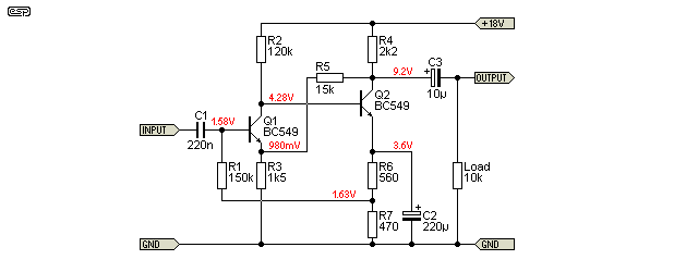
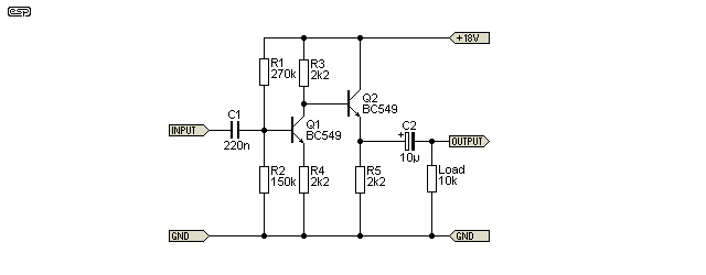
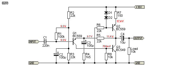
The following circuit uses two feedback networks. One is DC only, and sets the operating conditions via R1. The second feedback path is both AC and DC, and joins the emitter of Q1 to the collector of Q2. This second feedback path provides additional DC stability and sets the gain, which is (roughly) R5 / R3 (10.6 in this case). It should be closer to 11 (i.e. ( R5 / R3 ) +1 ), but the circuit has limited open-loop gain (about 2,600 as shown).
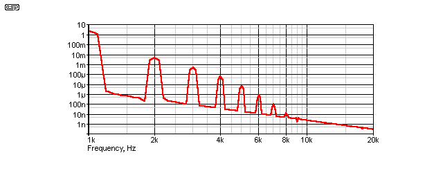
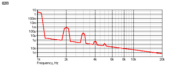
Under exactly the same drive conditions as Figure 1, this circuit has a distortion of 0.065%. The spectrum is shown below, using the same axes as Fig 2. It is very apparent that it has greatly reduced distortion. Although the harmonics do extend a little further than the first example, they are all well below the noise floor. This extension of the harmonics is not uncommon with feedback circuits, but when they are at such a low level it is of no consequence.
Another common variation shown in Figure 3b used one NPN and one PNP transistor. Performance is similar, but distortion may vary considerably depending on how it's biased. With the values given, a simulation says that distortion is 0.017%, and gain is 9.4 (19.5dB). Because the input transistor is biased from the supply, the complementary version is more susceptible to noise on the +18V rail. There used to be a number of variations, but most have fallen by the wayside over the years.
The dual NPN version is the better choice if you wanted to use this class of circuit. Another circuit that performs well is shown in Project 13. The disadvantage is that it's an inverting stage, and it has a comparatively low input impedance. For the same conditions, it's similar to the circuits shown above in terms of distortion, being around 0.015%.
What is most interesting is intermodulation performance of the dual NPN circuit (the NPN+PNP version is not included in this analysis) compared to a single transistor stage. Using the same criteria as in the first example, primary intermodulation products are at -63dB, 10dB lower than the simple amp in Figure 1. Since intermodulation is by far more irritating and obtrusive than harmonic distortion, it is important to minimise this wherever possible.
It is worth pointing out at this stage that a simulated TL072 amp (not regarded as an audiophile opamp by any means) will give intermodulation figures under identical operating conditions that are 96dB below the 1kHz or 9kHz levels. This is so much better than you will obtain with any of these circuits that it's just not worth considering them (IMO). However, I have started this article, and will continue to the bitter end.
The distortion components are reduced, and to make comparison easier, click on the above image to open it in a new window. Now, you can go back to Figure 2 and compare the two. Not so readily apparent is the fact that input impedance is much higher and output impedance much lower than a simple amplifier stage.
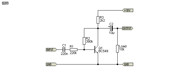
These are important parameters for audio (and indeed for all amplification circuits). The input impedance of the Fig 3a amp is around 145k - not much less than the value of the bias resistor (R1). The input impedance at the base of Q1 is about 4.6Meg with the circuit shown, and this is almost entirely due to the feedback (applied via R5 to the emitter of Q1). This feedback also defines the gain of the circuit, which is much closer to the design value (10 times, or 20dB). In theory, gain should be 11 - it can be worked out from ...
Av = ( R5 + R3 ) / R3 = ( 15k + 1.5k ) / 1.5k = 11 (Which can also be written as Av = ( R5 / R3 ) + 1 = 11 )
While it is easy to tweak the values to get the gain to exactly 10, in all cases in this examination we will be satisfied if it is within 3dB of the target. The circuit shown is a direct translation from the circuits presented in Reference 1 below.
Output impedance is harder to calculate than gain or input impedance, because you need to know the open loop gain of the amplifier. It was measured at about 39Ω, a vast improvement, and this means that sensible load impedances will not change the gain of the amplifier. It is very important to understand that the output impedance of any amplifier does not mean that it can drive that impedance.
I measured the open loop gain of the simulated dual-NPN circuit at 3,160 (70dB), so with a nominal gain of 10, there's about 50dB of feedback. Unlike an opamp, the open loop gain remains flat (-3dB) to over 60kHz. The open loop gain of the NPN/PNP circuit is 75dB, but otherwise the performance of both circuits is pretty much equal.
Particularly with resistor loaded circuits, the peak current available is determined by the output resistor - for the Fig 3a circuit, this means that it cannot supply more than 4mA peak into any load, and it is important that this is not exceeded. In fact, the current demanded by the load (be it a following amplifier stage, a volume control or external equipment) should be no more than ½ the peak current available to maintain linearity. Ideally, it will always be much less than this. For the circuit shown, the minimum suggested load is around 10k, although it will tolerate less if the peak output voltage swing is restricted to no more than (say) ±3-4V.
It is impractical to try to describe the design process for this circuit - not because it is hard, but because it is just time-consuming. Anyone who is interested enough can use the principles used in 2.2 to analyse the circuit. Despite the additional complexity, the basic analysis methods are the same.
This class of circuit pretty much sealed the fate of simple stages, and also entrenched the use of feedback as an indispensable tool to obtain improved performance with predictable results despite device parameter spread. Variations on these feedback amps were used for equalisers (especially RIAA phono and tape head preamps), microphone preamps, and a great many others.
Because of the tedious design process, Philips published a table of component values for different gains for the circuit of Fig. 3a, although they probably could have saved themselves some trouble with a fairly simple design modification. By partially bypassing R3 (using a resistor and capacitor in series) the gain is easily modified. I have reproduced the table below ...
| Component | 10dB Gain | 20dB Gain | 30dB Gain | 40dB Gain |
| R1 | 150k | 150k | 150k | 150k |
| R2 | 120k | 120k | 120k | 120k |
| R3 | 4.7k | 1.5k | 1.5k | 1k |
| R4 | 1.8k | 2.2k | 2.2k | 2.2k |
| R5 | 12k | 15k | 56k | 180k |
| R6 | 470R | 560R | 330R | 680R |
| R7 | 1.2k | 470R | 270R | 220R |
It is worth noting that there are two feedback loops in this design. One is DC only, and uses the voltage divider formed by R6 and R7. This biases the input transistor. The second feedback loop is via R5 and R3 - this is both AC and DC, so stabilises the DC operating conditions as well as the AC circuit gain.
All in all, this class of circuit was a breakthrough in the early days of transistor circuits, and I learned a great deal about the design process by analysing circuits such as this when I first became serious about electronics. That circuits such as this will never be the equal of one of today's opamps is readily apparent, but given the resurgence of people wanting to use discrete circuitry, someone will hopefully find this information interesting. Even today (after so many years of electronics) it is still fascinating to see the ways that were used to solve the problems that are inherent in all basic circuits.
Buffers were always a tricky issue before opamps, but the emitter follower ('common collector', because the collector is common for AC input and output) is probably one of the best known single transistor circuits known. It is still used to this day in some cases, and is perfectly ok where extreme precision is not needed. It is undoubtedly true that most opamps will have higher than expected distortion with high values of common mode voltage (the voltage that's common to both inputs). When used as a non-inverting buffer, opamps are run with the maximum possible common mode input voltage. However, distortion will still be far lower than most discrete circuits.
Emitter follower buffers can be improved considerably by using a current source in the emitter circuit, but this was very uncommon with early transistor circuits. While other (more complex) buffer circuits were sometimes used, this only applied for either seriously up-market applications, test equipment and some professional equipment.
There is a complete article that concentrates on buffers - see Voltage Followers And Buffers for the details. It covers these essential circuits in greater detail than you'll find here, although there is inevitably some overlap.
The emitter follower is non-inverting, has very good linearity for a simple circuit, but does not have unity gain. Typically, the gain is quoted as being between about 0.90 to 0.99, depending on the hFE of the transistor at the operating current (including current through the load resistance).
Figure 5 should be easily recognisable - this is a classic emitter follower. Gain is 0.98 and the circuit has low distortion at 0.059%. The highest intermodulation product is at -65dB (using the same parameters as before). While not as good as an opamp, these figures are fairly respectable, and the circuit is very cheap and almost infinitely reliable. The distortion spectrum is not shown, but is almost identical to that in Figure 4.
The emitter follower is the easiest transistor circuit to design, requiring the absolute minimum of maths to get a working circuit. Indeed, in most cases you can simply grab a handful of resistors, a transistor and a couple of caps and be in business. It is important to make sure that the emitter resistor is capable of supplying the current needed by the load, but this is usually as simple as making its value equal to around one fifth of the expected load impedance. For a load of 10k, that means a 2.2k resistor is fine.
Measurements of the Fig 5 circuit show that the input impedance at the base of Q1 is 390k. Assume a transistor hFE of 200 and an emitter current of about 3mA, so re is 26 / 3mA - just under 9Ω. The calculation for this is simply (and roughly) ...
Zb = (Ze + re) × hFE = 1.8k × 200 = 360k
Remember that re can be ignored if it is less than one tenth the value of the external load in parallel with the transistor's load resistance (now in the emitter circuit). Calculated and measured values are close enough. As before, total input impedance is ...
Zin = 1 / (1 / R1 + 1 / R2 + 1 / Zb) = 1 / (1 / 220k + 1 / 220k + 1 / 360k) = 84k
Output impedance is (approximately) equal to the total impedance seen by the base divided by the transistor's gain. This means that output impedance depends on the source impedance. This level of dependency affects all simple transistor circuits, where inputs are dependent on outputs or vice versa.
Although I have shown R1 and R2 as being equal values, in many cases it will be necessary to reduce the value of R1 to ensure that the emitter voltage is about half the supply voltage. With the values shown in Figure 5, the emitter voltage will only be about 7V, and R1 should be reduced to 180k to bring the voltage up to 9V (half the supply voltage).
It must be remembered that an emitter follower operates with 100% local feedback, and the circuit will become unstable if a reactive load (such as a capacitor or an un-terminated transmission line - shielded cable!) is connected to the output. I always recommend that a series resistor be used at the output of any emitter follower that will drive a cable that is more than 100mm long.
There is another thing that you need to be aware of. At high levels and low impedance loads, it's common for emitter follower circuits to clip prematurely and asymmetrically. The transistor can supply several milliamps easily, but the emitter resistor limits the current that can be drawn on negative half-cycles (Figure 5). For example, if the load is 2.2k (the same as R3), the maximum negative excursion is only about 3V because R3 can only sink a limited load current. If you recall, I stated that the emitter resistance should be around one fifth of the load impedance, so to drive a 2.2k load you need an emitter resistor of no more than 390Ω. Power dissipated in the resistor and transistor will be over 200mW.
This has caught people out many times, and you need to understand that when R3 is 2.2k, it can sink no more than 2mA before the voltage across it becomes high enough to cause clipping. For those who are used to opamps, the asymmetrical clipping behaviour with low impedance loads comes as a surprise. 2.2k is hardly a surprisingly low impedance, and can be driven by almost any opamp with ease, but not from a simple emitter follower unless the value of R3 is reduced. This will also decrease the input impedance, and will also require that R1 and R2 are reduced in value as well. The Figure 5B circuit addresses this to a degree, but the current source (Q2) has to be able to provide enough load current to prevent clipping with low impedances at the output.
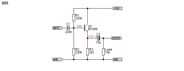
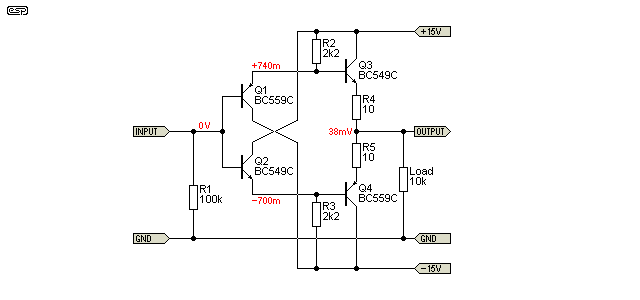
One very simple circuit is worthy of inclusion. This can only be used with low input levels, typically no more than 500mV peak (350mV RMS). It looks as if it couldn't possibly work, but it does, and may be useful. This input stage is used with some opamps that allow single supply operation with input voltages at (or near) zero. Surprisingly, the distortion is lower than the circuit shown in Figure 5. Its limitation is the low input voltage, but it's an interesting variation and is suitable for very low supply voltages (down to as low as 1.5V DC, but with reduced performance). Although it still has a high input impedance, the source should ideally be a fairly low impedance and earth referenced, or it will not work as well as it otherwise might. Also, be aware that a portion of the base current will flow in the source. If this is not acceptable, an input capacitor is needed which negates the advantage of the circuit's extreme simplicity. Use the highest gain possible for Q1.
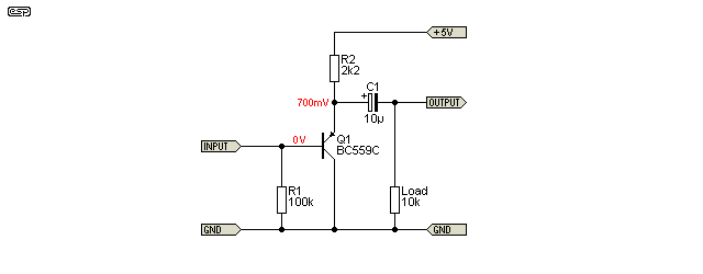
The circuit shown above has exemplary performance, almost rivalling the TL072 - at least in theory. DC offset at the output is very low and can be adjusted over a small range by changing the resistance of R2 (no less than 22k - lower values than shown cause negative offset and vice versa). The transistors used must be the highest gain variants you can get. BC549C/559C are shown, but other high gain transistors will also work.
As you can see from the circuit diagram, it's likely to cost more than an opamp, and will occupy more PCB real estate. Compared to a TL072, distortion is somewhat higher (about double) but is around half that of the simple single transistor version in Figure 5.
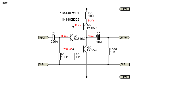
A buffer circuit that (based on some of the comments I've seen) has magical properties, is called the 'diamond' buffer. There is no magic of course, but it's significantly more complex than an opamp buffer and doesn't work quite as well. Gain is about 0.988 and distortion is below 0.001% as simulated. DC offset can only be minimised by matching the base-emitter voltage of the four transistors.
This is a very good circuit. There is little to criticise in terms of performance, and it started life as the (now obsolete) LH0002 IC from National Semiconductor. The IC was intended to be used within the feedback loop of an opamp to drive low impedance, high current loads (up to ±100mA steady state), although stand-alone applications also existed. For most audio applications, an opamp will beat a discrete version on most (if not all) counts, and will also cost less and use less PCB real estate. There is no magic, and it won't sound 'better' than an opamp, despite the claims you may see. DC offset may need to be trimmed in critical applications. This can be done by varying the value or R2 or R3, and the Vbe of the transistors should be matched carefully. There are countless variations on the basic circuit, with some being insanely complex - supposedly they sound 'better' (this is nonsense of course).
There are claims that audio equipment sounds 'better' if the circuit is capable of high output current. This is mainly for power amps, but also (presumably) extends to signal-level circuits. In general, a load will (and can) only draw the current demanded by its input impedance. A 1k impedance supplied with 1V needs 1mA - the ability to provide 100mA (for example) makes no difference whatsoever. However, some opamps cannot deliver their full performance driving loads much less than 2.2k or so. If that's what's needed, simply use a better opamp that can drive 600Ω loads.
There are many more things that could be said about emitter followers and non-inverting buffers, but this article is intended to cover the basics - if every variation were to be discussed it would become a book.
Inverting buffers are harder with discrete transistors without excessive circuit complexity. This rather paradoxical state of affairs occurs because of the very nature of the transistor and how it works, and the same issues were apparent with valve circuits. While a simple amp is inverting, a simple buffer (emitter follower) is non-inverting. It is possible to create an inverting buffer using the two circuits in tandem, as shown in Figure 6. No voltages are shown for these.
This circuit has many limitations, the main one being that voltage swing is rather limited. The absolute best that you can expect is about two thirds of the supply voltage (peak to peak), so for the circuit shown, about 12V P-P or 4V RMS. Assume that you will actually get less than this - the circuit above will only manage 3V RMS before clipping.
Because Q1 has the same resistor value for both collector and emitter, the voltages on each are essentially equal and opposite. The first stage therefore has unity gain, but inverted at the collector, while the emitter follower also has unity gain, but non-inverting. This circuit was common in valve amplifiers, as the basis for the 'split load' (aka 'concertina') phase splitter.
Another way that an inverting amp can be made is shown above. If the transistor had close to infinite gain, R1 and R2 would be equal values (as is normal with opamps), but in practice it's necessary to either reduce the value of R1 or increase the value of R2 to achieve unity gain and a reasonably symmetrical circuit. Ideally, the collector of Q1 should be at 9V DC with no signal, so it will usually be necessary to adjust R2 to obtain the proper DC characteristics, then R1 to obtain unity gain (but inverted of course).
One of the most irksome things about the circuit is the high resistances that are usually needed, as these increase noise. There are more complex arrangements that can be used so that more manageable resistance values can be used, but the circuit shown can never equal the performance of even a budget opamp. It does have the benefit of lots of negative feedback which keeps distortion fairly low, but output impedance is higher than one might hope for (about 680Ω for the circuit shown).
There are other alternatives, but inverting buffers were not common with early transistor equipment, and will not be covered any further here.
Simple transistor buffers are acceptable where one needs to provide a low output impedance with the minimum of fuss. The emitter follower is not good enough to use in accurate filters, as its gain of less than unity produces filters with a Q that is lower than expected, changing the filter characteristics.
The Figure 6 inverting buffer is a travesty - IMO it is next to useless in a transistor circuit unless the availability of a balanced output is necessary. This circuit was sometimes used to produce phase shift networks (but without the emitter follower stage). Given the limitations of the circuit, it is difficult to think of many areas where it might be used to advantage. The inverting buffer in Figure 6A is better in some respects, worse in others. If used with an emitter follower output it can work fairly well, but it's still limited.
By comparison, even a cheap opamp will outperform all of these circuits in almost every respect, and with fewer components,less PCB area and better power supply rejection. It would be silly to imagine that a simple discrete circuit could compete with modern opamps, some of which have distortion so low that special techniques are needed to measure it.
The original Baxandall feedback tone control was based on a simple amplification stage. It was used with both valve and transistor circuits, and although it certainly works, it also has some bad habits when used this way. Again, the problem is mainly one of distortion - with only a limited amount of gain available, there is inevitably more distortion than is usually considered acceptable.
Figure 7 shows the basic arrangement, but it must be admitted that there were a great many alternatives that performed far better than the circuit shown here. Again, it is impossible to give all the variants (or even a subset) because there are so many. All of the discrete versions have worse distortion characteristics than a similar circuit made using an opamp of reasonable specification.
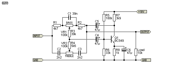
Distortion is only around 0.03% with the controls centred, and it manages to stay reasonably constant at 1kHz regardless of setting. At either frequency extreme things change radically though. Intermodulation rises dramatically at maximum treble cut or boost, with the first intermodulation products at -32dB below the 9kHz tone at either extreme. It must be considered that if the system has to be used with maximum treble boost or cut, then intermodulation is probably the least of your problems.
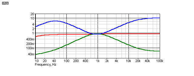
The response is shown above. It is quite obvious that there is much more treble boost (especially) than you will ever need (or hear), with the boosted signal extending to 100kHz and well beyond. Bass is reasonably well behaved, but with the peak boost at 42Hz, it needs to be extended to work with a system with a subwoofer. This can be done by increasing the value of C4 and C5. Frequencies are changed by using different capacitor values.
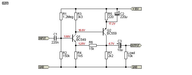
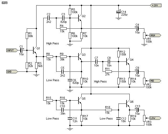
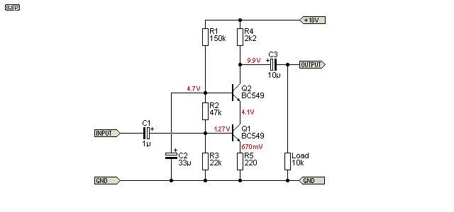
There is a lot to be said for discrete opamps - or at least circuits that have better performance than those looked at earlier in this article. With 0.024% THD and a very clean spectrum, the Project 37 amplifier is better than all of the alternatives shown previously. The main reason is the use of a current source (Q2) as the transistor load. Simply replacing Q2 with a 2.2k resistor increases THD to 0.25%.
To obtain the required gain (20dB), R5 had to be reduced to 1.5k - with 2.2k (theoretical gain of 11), the gain was well down from what it should have been. As we saw in previous examples, this is quite normal where the open loop gain is not high enough.
Although the circuit looks much more complex, it is only marginally worse in this respect than the circuit of Fig 3. The simple fact of the matter is that this level of performance is just not available from less complex circuits. As Einstein said, "All things should be as simple as possible, but no simpler". This is very true when it comes to circuits of this type, and in the author's opinion, far too many 'hi-if' amplifiers are much simpler than they should be. Equally, some are vastly more complex than they need to be, while giving little or no audible improvement. They may measure very well, but if you can't hear the difference there's not much point IMO.
The spectrum is shown below. This shows that the harmonic structure is almost entirely second and third harmonic, and even the third is at -98dB. This is negligible, so it is not unreasonable to claim that distortion is almost entirely second harmonic. The intermodulation results are even better - the first intermodulation product is at -72dB, almost 10dB better than the Fig 3 circuit, and nearly 20dB better than the simple amp in Fig 1.
The input impedance is about 96k - note the biasing arrangement, which is designed to minimise noise and maximise input impedance. C2 decouples any supply noise, and bias current is applied via R1. Q1's base input impedance is greater than 2.8 Meg, so R1 could be increased if desired.
It is fairly obvious that the small increase in complexity has yielded a large benefit - much lower distortion being the major improvement. This is particularly important for intermodulation distortion, and this is markedly improved from any of the alternatives. It's worth noting that it is exceptionally difficult to get this level of performance without using global negative feedback. While it is theoretically possible, it's generally impractical and just ends up costing a lot more for no tangible benefit.
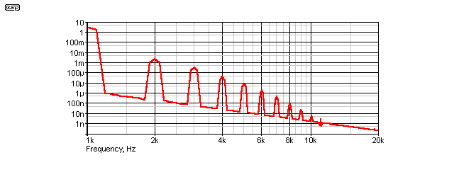
In amongst the more mundane voltage amplifier stages and other simple circuits, even from very early days people messed around with electronic crossover networks. I don't propose to cover those made using valves (vacuum tubes), but an early transistorised circuit came to my attention and I had to include it here. As published [ 4 ] the circuit had several mistakes and was quite clearly wrong in several respects. After basic corrections and a few minor circuit changes, the performance is still ... well ... atrocious!
It would certainly be possible to make it better, but emitter followers have a gain of slightly less than unity, so it can never equal the performance you'd expect from Project 09 for example. Don't expect to see a project based on this idea, because it will never happen and there is no point at all. Power supply rejection of the circuit below will be very poor indeed - expect no better than around 6dB. As a result, the supply needs to be very well filtered so the DC has no noise or ripple.
The circuit shown dates from the late 60s or early 70s. It's unknown if this was a commercial product or not, but I expect it probably was sold (although perhaps only in small numbers as electronic crossovers were uncommon at the time, and amplifiers were expensive). Note that 1nF caps from each emitter to earth have been omitted, as they would likely make any modern transistor oscillate. The original transistors specified were RCA 40232 - long obsolete.
The first stage is a simple emitter-follower buffer, which ensures a reasonably high input impedance and a low enough output impedance to drive the filters. Where possible, stages are direct coupled so that separate biasing resistors aren't needed for all of the emitter follower stages. Since all stages are emitter followers, distortion at normal levels should be quite low, but the output impedance of each stage is higher than ideal, and if loaded with a low impedance amplifier input, the filter response will change! Not by very much, but it will change. This is because the input impedance of an emitter follower is determined (in part at least) by the value of the emitter resistance and the external load (the two are effectively in parallel).
There is no attempt to try to ensure that phase shift is minimised, and the summed output peaks at almost 4.5dB at the crossover frequencies. The crossover frequencies are 390Hz and 4.37kHz with the values shown. It is possible to change the frequencies by scaling the appropriate resistors and caps. The filters originally used some non-standard caps which have been 'modernised' to use standard values. It is also notable that no inverter stage was used for the midrange output, so as shown the filters are out-of-phase. The midrange output requires inversion to maintain coherent phase across the 3 bands, but this wasn't included in the original design. It was expected that the phase of the midrange speaker would be reversed instead - not generally considered a good idea.
Although performance is very poor by modern standards, it is expected that even the circuit shown would out-perform most passive filters, and with a bit of tweaking it might even be passable today. Would I use it? No. Nor would I recommend anyone else do so. Opamp based filters are at least an order of magnitude better in all respects - filter accuracy, noise, distortion and drive capability. Because an opamp configured for unity gain really does have a gain of 1 (± a few parts per million) it will perform far better than an emitter follower with a typical gain of around 0.998 (assuming a high gain transistor).
In September 1971, John Linsley-Hood published an article in Wireless World, where he described a circuit he called the 'Liniac' (Linear Inverting Amplifier Circuit). The sub-heading was "A New Linear Inverting And Amplifying Circuit And Some Other Applications Of Low-level Darlington Transistors" [ 5 ]. The circuit was novel back then, and to some extent it still is. The claim was that it surpassed most of the existing topologies that were used at the time, and while it doesn't even come close to a TL072 in terms of distortion, with proper transistor selection it is capable of much lower noise than most common opamps. The µA709 was the first truly widely adopted monolithic opamp, followed by the venerable µA741 in 1968 [ 6 ]. However, the 741 was noisy and had very limited bandwidth. Countless magazines published audio circuits using it though, and it was common to add an external transistorised front-end to improve the noise characteristics.
The basic arrangement as originally described is shown below. It uses a JFET as a constant current source for the first transistor, and the output of the gain stage is buffered by a small-signal Darlington transistor. Because the collector load on the gain transistor is extremely high, it is capable of extraordinarily high gain. You can reasonably expect the gain from a single transistor (Q1) to exceed 67dB (about 2,500 times). Based on the description and FET information, the circuit shown is actually wrong - with an 82k resistor for R1, the collector current in Q2 will be a few microamps, and not 2-3mA as claimed in the article. R1 needs to be in the order of 2k2 to obtain a collector current of around 400µA in Q2 (it will vary with the FET used of course).
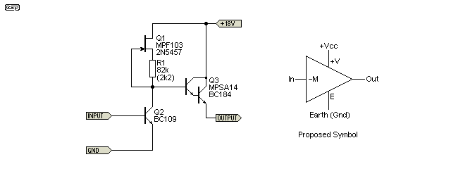
The original article describes multiple uses for the circuit, but here I will only show the basic implementation - an inverting gain stage with a gain of 47 (33.5dB). This shows the biasing circuit as shown in one of the designs in the article. Input impedance is 10k (set by R1) and the output impedance will be less than 10Ω with feedback applied. The symbol proposed by JLH is also shown. I imagine that he rather hoped that the circuit would become a standard, and perhaps even become an integrated circuit, but opamps quickly became available that were cheaper, easier to use, and had significantly better performance. As a result, Liniac circuits were few and far between.
With the arrangement shown above, I simulated the circuit with an input voltage of 10mV (peak), and obtained an output of 475mV (peak), a gain of 47.5 or 33.5dB. Distortion was 0.022%, and predictably this will decrease if the gain is reduced or increase as gain (or level) is increased. The values for R3 and R4 are taken from the original article, but are sub-optimal for maximum output swing. These resistors also affect the gain, because they form a voltage divider in the feedback path.
As a piece of history, the Liniac is interesting, but it has no place in modern designs unless there is a specific reason for using it that cannot be accomplished using an opamp. Despite not using any stabilisation capacitor, the high frequency response is somewhat limited (about 46kHz for the circuit shown above). Although improved high frequency performance can be achieved, in reality there's no point because it's already far greater than necessary for most audio applications. If operated at a reduced gain (such as -10 for example), the HF response extends to over 400kHz (-3dB frequency). One other important parameter - noise - was barely mentioned in the article, other than to state that it was 'low'.
When (depletion mode) JFETs first appeared, they were embraced by some as the ideal amplifying device. I suspect this was largely because they appealed to people who grew up with valves. They are biased in much the same way, and offered the familiar very high input impedance, low transconductance (compared to bipolar transistors) and similar characteristics, except they operated with low voltages. At one stage, there was a vast array of different devices readily available from small and large suppliers alike. This has dwindled to the point where there are few of the better devices on sale, although it's easy to get devices from the 'Far East' that claim to be the real McCoy but are usually fakes.
For example, the MPF103/ 2N5457 devices (and their close relatives) shown in the Liniac above used to be the mainstay of general-purpose JFET designs, but they are now obsolete and unavailable. There are still JFETs, but the range is now dismal. The situation is a great deal worse for specialised and especially very low noise types (e.g. 2SK170), and these have all but vanished.
The gain and linearity of JFETs is much worse than BJTs, and they have a wide parameter spread. Using the same brand and type never meant that the circuit was completely predictable, and if you did need a circuit to perform consistently in a production run, feedback, pre-selection or a trimpot was necessary to ensure that the circuit behaved in a predictable manner. However, the JFET has some unique advantages that can't be matched by other devices - including valves.
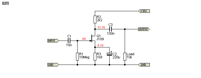
Probably the most important and useful property of the JFET is its input impedance. Unlike a valve, where extremely high value grid resistors can cause problems (see note below), a JFET is usually perfectly happy with a gate resistor of 1GΩ or more. In the circuit shown above, the JFET is biased by R3, and the bypass cap is necessary or the gain would be close to -1 (unity, but inverted).
In the circuit shown (with C2 in place), the gain as simulated is about 20 (26dB), and distortion is 1.8% - dramatically worse than the Figure 1A BJT circuit under the same conditions. This is not a good result. Of course, there are better JFETs than the J109 which is intended mainly for switching (typically in muting circuits and other signal switching applications), but any given JFET will normally have much higher distortion than a BJT under similar operating conditions.
Probably the greatest issue with JFETs is their parameter spread. A typical JFET (e.g. MPF102) may have a gate-source voltage of anything from -0.5V to -7.5V for a drain current of 200µA at 15V, and a drain current of between 2 and 20mA at zero gate voltage with respect to the source. This level of variation (a full order of magnitude) is unmatched by any other active device, and that's not a good thing. It means that you have to accept wide variations in operating conditions for a given set of resistor values, and if predictable performance is needed you need to include a trimpot or select the devices before they are used. I have used JFETs in a couple of published designs, but only because there was no alternative for high impedance input circuits having the bandwidth needed (an example is Project 16 Audio Millivoltmeter).
Switching MOSFETs (enhancement mode HEXFETs or 'vertical' MOSFETs in general) are also used in some cases. High voltage types make surprisingly good followers in valve equipment, but as small signal amplifiers MOSFETs are usually rather disappointing. Noise is higher than BJTs or most JFETs, and their parameter spread is usually rather large. Distortion is typically similar to that obtained from single JFET, but their higher gain (transconductance) means that source degeneration (local feedback) can be applied. Distortion will still be greater than a single BJT amplifier for the same conditions. Overall, this is not an approach I'd recommend for any linear circuit, because MOSFETs simply are not as linear as BJTs. Accordingly, no schematic is shown, because performance is so poor.
Note: It's commonly believed that valves have almost infinite input impedance, but the grid will 'collect' electrons, and if there is no leakage path the valve may bias itself almost to cutoff (zero plate current). This phenomenon was used for what was called 'grid leak' bias, where a resistor between 2MΩ and 10MΩ was used in lieu of a cathode bias resistor. Consequently, if very high input impedance was needed with a valve, it commonly meant specialised circuitry or a valve that was designed for the job. However, cathode followers are fairly tolerant of very high input impedances. A JFET does not have this problem at all.
The cascode arrangement is common for RF circuits, less so for audio. There may be some people who insist that cascode 'sounds better' (whatever that's supposed to mean), but it's safe to say that's not the case. There is some conjecture as to the origin of the term 'cascode', but you can think of it as 'cascaded electrode'. The circuit was invented during the valve (vacuum tube) era (in around 1939), and used a pair of triodes, the first as common cathode and the second as common grid. A pentode achieves a similar result by having the screen grid grounded for AC, at least partially eliminating plate-to-grid feedback.
I used the same basic arrangement as shown in Fig. 1, with the same biasing for the input transistor. The second transistor operates as common-base, with the input applied to its emitter. Because the base of Q2 is grounded for the signal (via C2), stray capacitance from collector to base is eliminated. Since Q1 feeds a very low impedance (less than 10Ω), there is no signal present at the collector of Q1, so feedback to the base is effectively eliminated. The Miller effect is therefore all but defeated, as there is no intrinsic capacitance between the input and output.
Compared to the Fig. 1 circuit, the cascode circuit can have a bandwidth that's improved by up to an order of magnitude (depending on the source impedance). With a source impedance of 10k, the bandwidth is improved from 1.4MHz to 5.6MHz compared to Fig. 1 (as simulated). The cascode circuit can be equipped with an emitter follower for reduced output impedance like any other stage. Although this circuit has little to do with a comparison between discrete circuits and opamps, it's still useful, and (IMO) important enough to include. (Mind you, it did take 20 years for me to add it, but better late than never .)
Cascode circuits can also use JFETs or MOSFETs, either exclusively or in combination with a BJT. A common arrangement is to use a JFET for the input (Q1) and a BJT for Q2. This provides a very high input impedance thanks to the JFET. It's possible to get high gain and wide bandwidth using a hybrid JFET/ BJT cascode. In most cases this is the best option, but of course JFETs have a wide parameter spread so the source resistor may need to be a trimpot to set the operating conditions.
The circuit shown is not optimised, but the voltages shown on the drawing are 'reasonable'. A major part of the design process is to ensure that both transistors have a voltage across them, with neither device saturated (turned on fully). Q1 has a collector-emitter voltage of 3.4V, with the collector voltage remaining steady at 4.1V. The emitter voltage does vary, as it essentially follows the input voltage unless R5 is bypassed. Ideally, the collector of Q2 will be at 11V for maximum undistorted output. I don't intend to provide the full design process, as it's unlikely that you'll ever need a cascode circuit in any audio projects, but there's a wealth of information on-line if you wish to pursue the circuit in greater detail.
From the details here, it's obvious that it is difficult to obtain good performance from simple discrete circuits. While improved versions (such as the P37 preamp we looked at in section 5) do perform very well, in general the 'old' circuits do not. They were a triumph in their day, but those days are well behind us. I haven't covered the many and various more complex designs that have been used over the years, and some are still used in some cases because there are people who believe there are 'flaws' in opamp circuits that measurements fail to reveal. I consider this to be nonsense.
The 'advanced' two-transistor (with feedback) circuits were certainly an enormous improvement over simple one-transistor designs. However, modern opamps are so superior that there is no reason to look elsewhere, unless you wish to experiment and learn more about the design processes involved. While there is certainly some historical value in the circuits shown, they are no longer to the standard expected of true high fidelity.
I haven't gone into details about intermodulation distortion, but the presence of harmonic distortion means that intermodulation distortion is inevitable. Where the simulator shows that the first intermodulation product using a TL072 is 109dB below the 9kHz tone, none of the circuits shown come even close to this. The P37 amp is certainly better than any of the others, but it is still not as good as a good opamp. It is probable that the intermodulation from P37 is inaudible (after all, many people have commented on just how good it sounds), and it is equally probable that the simulator over-estimated the TL072's quality - it is a simulator, after all. I ran a new intermodulation test using an LM358 opamp (hardly a renowned device for audio), and SIMetrix said that intermodulation distortion was at -68dB. From that, we can deduce that the models are reasonable so the simulated results will not be too far from reality. Of course there are many opamps that are vastly superior to the TL072.
There is no doubt that modern devices such as the LM4562, OPA2134 or the venerable NE5534 (or the dual version, NE5532) will be much better than anything shown here, but will they sound as good, better or worse? This is something that can only be determined with a proper blind AB test. In general, most opamps provide frequency response that can't be faulted - ruler flat from DC to at least 100kHz with gains of 20 or less, with almost immeasurably low levels of distortion, both harmonic and intermodulation. Logically, it should not be possible to hear the difference between any decent opamps, or even the P37 circuit. As for the others ... I don't know, but if you ever find out, be sure to let me know.
1. SIMetrix SIMetrix circuit simulator (UK)
2. Audio Amplifier Systems Philips Application Book , MD Hull, Third Edition, June 1972
3. Project 37 Elliott Sound Products , Rod Elliott, November 1999
4. Audio Cylopedia, Howard M Tremaine, pp 1125..1127 - 3-Channel Electronic Crossover Using Transistors (C.G. McProud)
5. The Liniac, John L Linsley-Hood - Wireless World, September 1971
6. Operational Amplifier - Historical Timeline (Wikipedia)
| Main Index
Articles Index
|